Understanding Timing Parameters in Nand Flash Controller
The NAND flash used in mini2440 is from Samsung, the part number is K9F2G08U0C, the meaning of it is defined in Samsung Part Number Decoder, we can get the basic information from it, but, right now, I am not interest in this kind of information, the crucial part for software is timing, before dive into it, let’s get familiar with the signals used in NAND flash, the follow table is taken from the datasheet of K9F2G08U0:
| Pin | Function |
|---|---|
| CLE | COMMAND LATCH ENABLE The CLE input controls the activating path for commands sent to the command register. When active high, commands are latched into the command register through the I/O ports on the rising edge of the nWE signal. |
| ALE | ADDRESS LATCH ENABLE The ALE input controls the activating path for address to the internal address registers. Addresses are latched on the rising edge of nWE with ALE high. |
| nCE | CHIP ENABLE The nCE input is the device selection control. When the device is in the Busy state, nCE high is ignored, and the device does not return to standby mode in program or erase operation. |
| nRE | READ ENABLE The nRE input is the serial data-out control, and when active drives the data onto the I/O bus. Data is valid tREA after the falling edge of nRE which also increments the internal column address counter by one. |
| nWE | WRITE ENABLE The nWE input controls writes to the I/O port. Commands, address and data are latched on the rising edge of the nWE pulse. |
| nWP | WRITE PROTECT The nWP pin provides inadvertent program/erase protection during power transitions. The internal high voltage generator is reset when the nWP pin is active low. |
| R/B | READY/BUSY OUTPUT The R/B output indicates the status of the device operation. When low, it indicates that a program, erase or random read operation is in process and returns to high state upon completion. It is an open drain output and does not float to high-z condition when the chip is deselected or when outputs are disabled. |
The timing information related to NAND flash control setup is as follows:
| Parameter | Symbol | Min (3.3V) | Unit |
|---|---|---|---|
| CLE Setup Time | tCLS | 12 | ns |
| ALE Setup Time | tALS | 12 | ns |
| ALE Hold Time | tALH | 5 | ns |
| CLE Hold Time | tCLH | 5 | ns |
| nWE Pulse Time | tWP | 12 | ns |
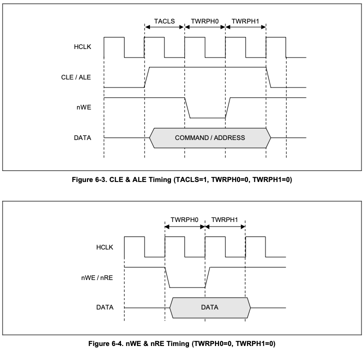
There are only three configurable parameters in NAND flash configuration register of S3C2440:
| NFCONF | Bit | Description | Initial State |
|---|---|---|---|
| Reserved | [15:14] | Reserved | – |
| TACLS | [13:12] | CLE & ALE duration setting value (0~3) Duration = HCLK x TACLS |
01 |
| Reserved | [11] | Reserved | 0 |
| TWRPH0 | [10:8] | TWRPH0 duration setting value (0~7) Duration= HCLKx(TWRPH0+1) |
000 |
| Reserved | [7] | Reserved | 0 |
| TWRPH1 | [6:4] | TWRPH1 duration setting value (0~7) Duration= HCLKx(TWRPH1+1) |
000 |
The ALE and CLE timing are similar so there is only one figure for this:
 I guess the
 S in TACLS means setup, A and C means ALE and CLE respectively,
so the TACLS means ALE/CLE setup time.
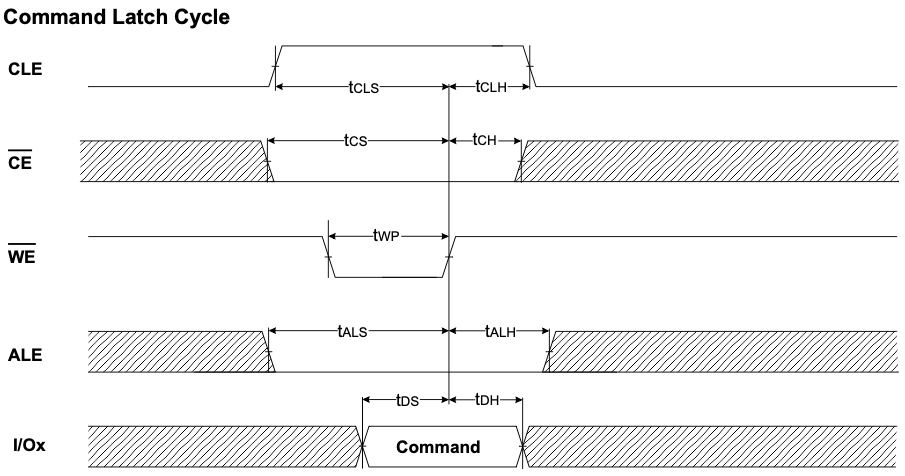
This is a little different from the definition of CLE/ALE setup time in command
latch cycle described in datasheet:
tWP is included in tCLS, so for the TACLS field in NFCONF, TACLS=tCLS-tWP, here the HCLK is 101.25 MHz, so 1 HCLK is around 9.877(1000/101.25)ns
TACLS = tCLS - tWP = 12 - 12 = 0
TWRPH0 is easy to confirm, it is nWE Pulse Width (tWP) tWP = 12ns, this is the minimum value, so higher than this is acceptable, if set it to two times of HCLK, then
TWRPH0 = 2HCLK/HCLK - 1 = 1
TWRPH1 is CLE Hold Time (tCLH) tCLH = 5ns, twice this value to 10ns
TWRPH1 = 10/HCLK - 1 = 0
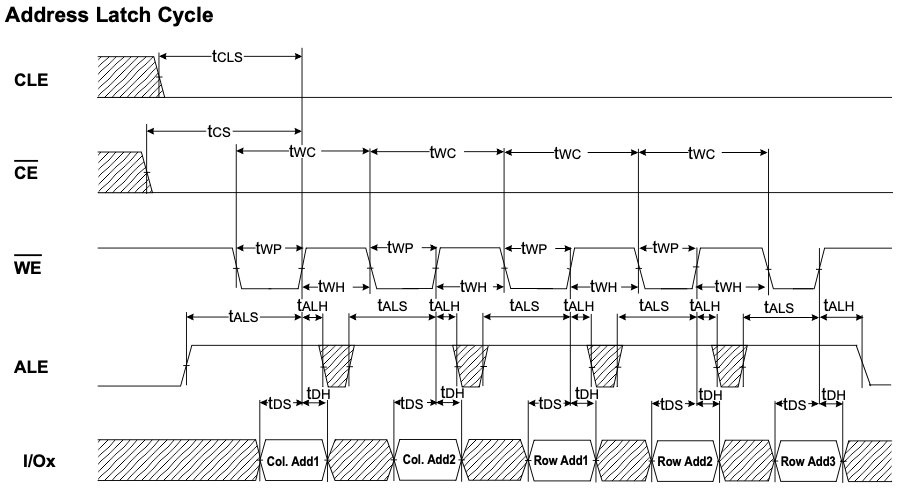
ALE and CLE are similar, put the timing of address latch cycle here for reference: