
U-Boot: Understanding Start.S
U-Boot is a universal bootloader for many architectures, the U-Boot image build against current version (u-boot-2020.10) cannot fit the size of stepping zone of S3C2440 (4KB), and using SPL (Secondary Program Loader) seems to be a choice to make it works.
_start
From 5a8ba3, the most of s3c24x0 related code were dropped from mainline, I copied those missing code from u-boot-2017.05, and make SPL works, this post gonna talk about boot process of U-Boot SPL.
The main entry point of U-Boot is defined in arch/arm/cpu/u-boot-spl.lds:
ENTRY(_start)
_start is a global symbol defined in arch/arm/lib/vectors.S:
.globl _start

_start:
	ARM_VECTORS
And ARM_VECTORS is actually a macro also defined in this file:
	.macro ARM_VECTORS
	b	reset
	ldr	pc, _undefined_instruction
	ldr	pc, _software_interrupt
	ldr	pc, _prefetch_abort
	ldr	pc, _data_abort
	ldr	pc, _not_used
	ldr	pc, _irq
	ldr	pc, _fiq
	.endm
These are exception vectors which can be found in S3C2440’s user manual:
Table 2-3. Exception Vectors
| Address | Exception | Mode in Entry |
|---|---|---|
| 0x00000000 | Reset | Supervisor |
| 0x00000004 | Undefined instruction | Undefined |
| 0x00000008 | Software Interrupt | Supervisor |
| 0x0000000C | Abort (prefetch) | Abort |
| 0x00000010 | Abort (data) | Abort |
| 0x00000014 | Reserved | Reserved |
| 0x00000018 | IRQ | IRQ |
| 0x0000001C | FIQ | FIQ |
The first instruction in ARM_VECTORS is b reset which goes to start.S for
s3c2440, it is arch/arm/cpu/arm920t/start.S.
| Mnemonic | Instruction | Action |
|---|---|---|
| B | Branch | R15: = address |
You can find the address of reset in spl/u-boot-spl.map:
 arch/arm/cpu/arm920t/start.o(.text*)
 .text          0x0000000000000044       0x7c arch/arm/cpu/arm920t/start.o
                0x0000000000000044                reset
R15 is Program Counter (PC), we step in gdb can see the change, which is highlighted
in Registers section:
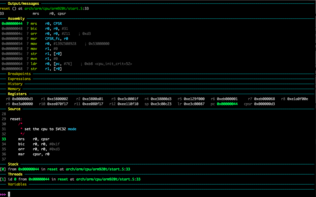 And the instruction to be executed is also highlighted in both
 Assembly and
Source section.
It may require below command to show registers correctly:
dashboard registers -style list 'r0 r1 r2 r3 r4 r5 r6 r7 r8 r9 r10 r11 r12 sp lr pc cpsr'
I am using gdb-dashboard for gdb debugging BTW.
Reset
Here is the reset flow for S3C2440:
When the nRESET signal goes LOW, ARM920T abandons the executing instruction and
then continues to fetch instructions from incrementing word addresses.
When nRESET goes HIGH again, ARM920T:
- Overwrites R14_svc and SPSR_svc by copying the current values of the PC and
CPSR into them. The value of the saved PC and SPSR is not defined.- Forces M[4:0] to 10011 (Supervisor mode), sets the I and F bits in the CPSR,
and clears the CPSR’s T bit.- Forces the PC to fetch the next instruction from address 0x00.
- Execution resumes in ARM state.
Before dive into the reset code, first let’s take a look at the bit definition of
CPSR (Current Program Status Register):
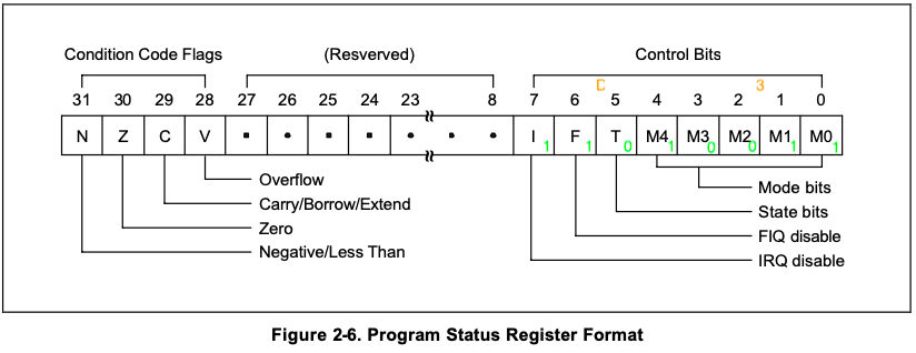
| The T bit | This reflects the operating state. When this bit is set, the processor is executed in THUMB state, or otherwise it is executing in ARM state. This is reflected on the TBIT external signal. Note: That the software must never change the state of the TBIT in the CPSR. If this happens, the processor will enter an unpredictable state. |
| Interrupt disable bits | I and F bits are the interrupt disable bits. When set, these disable the IRQ and FIQ interrupts respectively. |
| The mode bits | The M4, M3, M2, M1 and M0 bits (M[4:0]) are the mode bits. These determine the processor’s operating mode, as shown in Table 2-1. Not all combinations of the mode bits define a valid processor mode. Only those explicitly described shall be used. The user should be aware that if any illegal value is programmed into the mode bits, M[4:0], then the processor will enter an unrecoverable state. If this occurs, reset should be applied. |
| Reserved bits | The remaining bits in the PSRs are reserved. When changing a PSR’s flag or control bits, you must ensure that these unused bits are not altered. Also, your program should not rely on them containing specific values, since in future processors they may read as one or zero. |
I’ve noticed there is a confliction in the reset flow and the T bit definition: the reset flow clears the T bit, and the T bit definition says change the state of the TBIT will make processor enter an unpredictable state, but clearing this bit actually works in U-Boot.
Now let’s see the code, reset part in arch/arm/cpu/arm920t/start.S does what’s
required to do:
- M[4:0] = 10011
- set I,F bits
- Clear T bit
	.globl	reset

reset:
	/*
	 * set the cpu to SVC32 mode
	 */
	mrs	r0, cpsr
	bic	r0, r0, #0x1f
	orr	r0, r0, #0xd3
	msr	cpsr, r0
The instructions used in reset:
| Mnemonic | Instruction | Action |
|---|---|---|
| MRS | Move PSR status/flags to register | Rn: = PSR |
| MSR | Move register to PSR status/flags | PSR: = Rm |
| BIC | Bit clear | Rd: = Rn AND NOT Op2 |
| ORR | OR | Rd: = Rn OR Op2 |
Turn off watchdog and disable interrupts
The watchdog must be disabled, otherwise reset signal is activated for 128 PCLK cycles when the timer count value reaches 0:
#  define pWTCON	0x53000000
	ldr	r0, =pWTCON       @ r0=0x53000000
	mov	r1, #0x0          @ r1=0x0
	str	r1, [r0]          @ *(0x53000000) = 0x0
We don’t want any interrupts, so mask them all:
#  define INTMSK	0x4A000008	/* Interrupt-Controller base addresses */
#  define INTSUBMSK	0x4A00001C
#  define vINSUBTMSK	0x7FFF

	mov	r1, #0xffffffff
	ldr	r0, =INTMSK
	str	r1, [r0]

	ldr	r1, =vINTSUBMSK
	ldr	r0, =INTSUBMSK
	str	r1, [r0]
NOTE: S3C2440 actually have 15 bits in INTSUBMSK register, which can be found in
INTERRUPT SUB MASK (INTSUBMSK) REGISTER section of Chapter 14 (page 395).
| Mnemonic | Instruction | Action |
|---|---|---|
| MOV | Move register or constant | Rd: = Op2 |
| LDR | Load register from memory | Rd: = (address) |
| STR | Store register to memory | <address>: = Rd |
Setup CPU Clocks
There are 3 clocks used in S3C2440, they are:
- FCLK is used by ARM920T.
- HCLK is used for AHB bus, which is used by the ARM920T, the memory controller, the interrupt controller, the LCD controller, the DMA and USB host block.
- PCLK is used for APB bus, which is used by the peripherals such as WDT, IIS, I2C, PWM timer, MMC interface, ADC, UART, GPIO, RTC and SPI.
The registers involved for setting CPU clock is PLLCON, CLKDIVN and CAMDIVN, these are extracted from the user manual:
PLL CONTROL REGISTER (MPLLCON &UPLLCON)
| Register | Address | R/W | Description | Reset Value |
|---|---|---|---|---|
| MPLLCON | 0x4C000004 | R/W | MPLL configuration register | 0x00096030 |
| UPLLCON | 0x4C000008 | R/W | UPLL configuration register | 0x0004d030 |
| PLLCON | Bit | Description | Initial State |
|---|---|---|---|
| MDIV | [19:12] | Main divider control | 0x96 / 0x4d |
| PDIV | [9:4] | Pre-divider control | 0x03 / 0x03 |
| SDIV | [1:0] | Post divider control | 0x0 / 0x0 |
NOTE:
When you set MPLL&UPLL values, you have to set the UPLL value first and then the
MPLL value. (Needs intervals approximately 7 NOP)
Take MPLL Control Register for example, the output frequency (Mpll) can be calculated by the following formula:
Mpll = (2 * m * Fin) / (p * 2S)
m = (MDIV + 8)
p = (PDIV + 2)
s = SDIV
Suppose we want output frequency to be 405 MHz, then
m = 0x7f + 8
p = 2 + 2
s = 1
Fin = 12 MHz
Mpll = 405 MHz = (2 * 135 * 12) / (4 * 2)
Samsung recommend only use the values in below table:
PLL VALUE SELECTION TABLE
| Input Frequency | Output Frequency | MDIV | PDIV | SDIV |
|---|---|---|---|---|
| 12.0000MHz | 48.00 MHz (Note) | 56(0x38) | 2 | 2 |
| 12.0000MHz | 96.00 MHz (Note) | 56(0x38) | 2 | 1 |
| 12.0000MHz | 271.50 MHz | 173(0xad) | 2 | 2 |
| 12.0000MHz | 304.00 MHz | 68(0x44) | 1 | 1 |
| 12.0000MHz | 405.00 MHz | 127(0x7f) | 2 | 1 |
| 12.0000MHz | 532.00 MHz | 125(0x7d) | 1 | 1 |
NOTE: The 48.00MHz and 96MHz output is used for UPLLCON register.
You can choose your own value set by applying the following rules, but it is not
recommended:
PLL Value Selection Guide (MPLLCON)
- FOUT=2 * m * Fin/(p * 2S), FVCO=2 * m * Fin/p where: m=MDIV+8, p=PDIV+2, s=SDIV
- 600MHz ≤ FVCO ≤ 1.2GHz
- 200MHz ≤ FCLKOUT ≤ 600MHz
- Don’t set the P or M value as zero
- The proper range of P and M: 1 ≤ P ≤ 62, 1 ≤ M ≤ 248
| Parameter | Value |
|---|---|
| Max. Operating frequency (FCLK) | 400 MHz |
| Max. Operating frequency (HCLK) | 133 MHz |
| Max. Operating frequency (PCLK) | 67 MHz |
For mini2440, I want to run at 405 MHz, the related code as follows:
#  define MPLLCON	0x4C000004
#  define M_MDIV	(0x7F << 12)
#  define M_PDIV	(0x02 << 4)
#  define M_SDIV	(0x01 << 0)
#  define MPLL		(M_MDIV | M_PDIV | M_SDIV)

	ldr	r0, =MPLLCON
	ldr	r1, =MPLL
	str	r1, [r0]
CLKDIVN defines ratio between FCLK, HCLK and PCLK.
CLOCK DIVIDER CONTROL (CLKDIVN) REGISTER
| Register | Address | R/W | Description | Reset Value |
|---|---|---|---|---|
| CLKDIVN | 0x4C000014 | R/W | Clock divider control register | 0x00000000 |
| CLKDIVN | Bit | Description | Initial State |
|---|---|---|---|
| DIVN_UPLL | [3] | UCLK select register(UCLK must be 48MHz for USB) 0: UCLK = UPLL clock 1: UCLK = UPLL clock / 2 Set to 0, when UPLL clock is set as 48MHz Set to 1. when UPLL clock is set as 96MHz. |
0 |
| HDIVN | [2:1] | 00 : HCLK = FCLK/1. 01 : HCLK = FCLK/2. 10 : HCLK = FCLK/4 when CAMDIVN[9] = 0. HCLK= FCLK/8 when CAMDIVN[9] = 1. 11 : HCLK = FCLK/3 when CAMDIVN[8] = 0. HCLK = FCLK/6 when CAMDIVN[8] = 1. |
00 |
| PDIVN | [0] | 0: PCLK has the clock same as the HCLK/1. 1: PCLK has the clock same as the HCLK/2. |
0 |
CAMDIVN can leave untouched to use its default value.
The FCLK:HCLK:PCLK radio is set to 1:4:8:
#  define CLKDIVN	0x4C000014	/* clock divisor register */
#  define CAMDIVN	0x4C000018	/* Camera clock divider register */

	ldr	r0, =CLKDIVN
	mov	r1, #5
	str	r1, [r0]

	/* FCLK:HCLK = 1:4 */
	ldr	r0, =CAMDIVN
	mov	r1, #0
	str	r1, [r0]
CPU Critical Initialization
This is the final part of start.S, including cpu_init_crit and memory timing
setup, the latter one will be in a separate post.
#ifndef CONFIG_SKIP_LOWLEVEL_INIT
	bl	cpu_init_crit
#endif
This will branch to cpu_init_crit and return back when it finishes, so branch
with link was used.
| Mnemonic | Instruction | Action |
|---|---|---|
| BL | Branch with link | R14: = R15, R15: = address |
Invalidate I/D Caches and TLBs
Invalidating Caches and TLBs are done with CP15 registers, including:
- Register 1, control register
- Register 7, cache operations register
- Register 8, TLB (Translation Lookaside Buffer) operations register
Register 7 and 8 are write-only registers, only relevant part is excerpted from ARM920T Technical Reference Manual(hereafter this will be referenced as ARM920T manual).
Register 7 is used to manage the ICache and DCache.
| Function | Data | Instruction |
|---|---|---|
| Invalidate ICache and DCache | SBZ | MCR p15, 0, Rd, c7, c7, 0 |
| Invalidate ICache | SBZ | MCR p15, 0, Rd, c7, c5, 0 |
| Invalidate DCache | SBZ | MCR p15, 0, Rd, c7, c6, 0 |
Register 8 is used to manage the instruction TLB, and the data TLB.
| Function | Data | Instruction |
|---|---|---|
| Invalidate TLB(s) | SBZ | MCR p15, 0, Rd, c8, c7, 0 |
| Invalidate I TLB | SBZ | MCR p15, 0, Rd, c8, c5, 0 |
| Invalidate D TLB | SBZ | MCR p15, 0, Rd, c8, c6, 0 |
SBZ means Should Be Zero that is: when writing to this location, all bits of this field should be 0.
#ifndef CONFIG_SKIP_LOWLEVEL_INIT
cpu_init_crit:
	mov	r0, #0
	mcr	p15, 0, r0, c7, c7, 0	/* flush v3/v4 cache */
	mcr	p15, 0, r0, c8, c7, 0	/* flush v4 TLB */
According to the manual the comment is incorrect it should be invalidate, not flush.
Disable MMU stuff and caches
The control register controls arm920t feature on/off, each feature corresponds to one bit in this register, write to this register should follow read-modify-write fashion with the following instructions:
MRC p15, 0, Rd, c1, c0, 0 ; read control register
MCR p15, 0, Rd, c1, c0, 0 ; write control register
Below is the bit definitions for control register 1:
| Register bits | Name | Function | Value |
|---|---|---|---|
| 31 | iA bit | Asynchronous clock select | See below: Clocking modes |
| 30 | nF bit | notFastBus select | See below: Clocking modes |
| 29:15 | - | Reserved | Read = Unpredictable. Write = Should be zero. |
| 14 | RR bit | Round robin replacement | 0 = Random replacement. 1 = Round-robin replacement. |
| 13 | V bit | Base location of exception registers | 0 = Low addresses = 0x00000000. 1 = High addresses = 0xFFFF0000. |
| 12 | I bit | ICache enable | 0 = ICache disabled. 1 = ICache enabled. |
| 11:10 | - | Reserved | Read = 00. Write = 00. |
| 9 | R bit | ROM protection | This bit modifies the MMU protection system. See Domain access control on page 3-23. |
| 8 | S bit | System protection | This bit modifies the MMU protection system. See Domain access control on page 3-23. |
| 7 | B bit | Endianness | 0 = Little-endian operation. 1 = Big-endian operation. |
| 6:3 | - | Reserved | Read = 1111. Write = 1111. |
| 2 | C bit | DCache enable | 0 = DCache disabled. 1 = DCache enabled. |
| 1 | A bit | Alignment fault enable | Data address alignment fault checking. 0 = Fault checking disabled. 1 = Fault checking enabled. |
| 0 | M bit | MMU enable | 0 = MMU disabled. 1 = MMU enabled. |
Clocking modes
| Clocking mode | iA | nF |
|---|---|---|
| FastBus mode | 0 | 0 |
| Synchronous | 0 | 1 |
| Reserved | 1 | 0 |
| Asynchronous | 1 | 1 |
	mrc	p15, 0, r0, c1, c0, 0
	bic	r0, r0, #0x00002300	@ clear bits 13, 9:8 (--V- --RS)
	bic	r0, r0, #0x00000087	@ clear bits 7, 2:0 (B--- -CAM)
	orr	r0, r0, #0x00000002	@ set bit 2 (A) Align
	orr	r0, r0, #0x00001000	@ set bit 12 (I) I-Cache
	mcr	p15, 0, r0, c1, c0, 0
| Mnemonic | Instruction | Action |
|---|---|---|
| BIC | Bit clear | Rd: = Rn AND NOT Op2 |
| MCR | Move CPU register to coprocessor register | cRn: = rRn { |
| MRC | Move from coprocessor register to CPU register | Rn: = cRn { |
| ORR | OR | Rd: = Rn OR Op2 |
Memory timing setup in lowlevel_init
After cpu_init_crit we need to get back and keep going in the main routine, the
return address is saved to lr with bl, now we need to go to lowlevel_init, also
with bl, the original value saved in lr will be overwritten, so we save it to
ip, and move back when lowlevel_init completed:
#ifndef CONFIG_SKIP_LOWLEVEL_INIT_ONLY
	mov	ip, lr
	bl	lowlevel_init
	mov	lr, ip
#endif
	mov	pc, lr
#endif /* CONFIG_SKIP_LOWLEVEL_INIT */
In gdb Assembly window you will see mov r12, lr instead of mov ip, lr,
it’s the same, r12 act as Intra Procedure call scratch Register.
Troubleshooting
Cannot show Register correctly
Q: After connect to gdb server (OpenOCD) with:
target extended-remote localhost:3333
The Registers section of gdb-dashboard show the following error:
Traceback (most recent call last):
  File "<string>", line 538, in render
  File "<string>", line 1940, in lines
ValueError: max() arg is an empty sequence
A: Found the solution from this issue: This is needed for some architectures and it’s a GDB limitation AFACT, for example:
dashboard registers -style list 'r0 r1 r2 r3 r4 r5 r6 r7 r8 r9 r10 r11 r12 sp lr pc cpsr'